Definition:
Transistors are three terminal active devices made from different semiconductor materials that can act as either an insulator or a conductor by the application of a small signal voltage. The transistor's ability to change between these two states enables it to have two basic functions: "switching" (digital electronics) or "amplification" (analogue electronics).Construction:
-The Bipolar Transistor basic construction consists of two PN-junctions producing three connecting terminals with each terminal being given a name to identify it from the other two. These three terminals are known and labelled as the Emitter (E), the Base (B) and the Collector (C) respectively.
-Bipolar Transistors are current regulating devices that control the amount of current flowing through them in proportion to the amount of biasing voltage applied to their base terminal acting like a current-controlled switch. The principle of operation of the two transistor types NPN and PNP, is exactly the same the only difference being in their biasing and the polarity of the power supply for each type.

Transistor configuration:
1. Common Base Configuration - has Voltage Gain but no Current Gain.
2. Common Emitter Configuration - has both Current and Voltage Gain.
3. Common Collector Configuration - has Current Gain but no Voltage Gain.
Common Base Configuration: CB
In the Common Base or grounded base configuration, the BASE connection is common to both the input signal AND the output signal with the input signal being applied between the base and the emitter terminals. The corresponding output signal is taken from between the base and the collector terminals as shown with the base terminal grounded or connected to a fixed reference voltage point. The input current flowing into the emitter is quite large as its the sum of both the base current and collector current respectively therefore, the collector current output is less than the emitter current input resulting in a current gain for this type of circuit of "1" (unity) or less, in other words the common base configuration "attenuates" the input signal.

This type of amplifier configuration is a non-inverting voltage amplifier circuit, in that the signal voltages Vin and Vout are in-phase. This type of transistor arrangement is not very common due to its unusually high voltage gain characteristics. Its output characteristics represent that of a forward biased diode while the input characteristics represent that of an illuminated photo-diode. Also this type of bipolar transistor configuration has a high ratio of output to input resistance or more importantly "load" resistance (RL) to "input" resistance (Rin) giving it a value of "Resistance Gain". Then the voltage gain (Av for a common base configuration is therefore given as:
Common base voltage gain:

Common Emitter Configuration:

In the Common Emitter or grounded emitter configuration, the input signal is applied between the base, while the output is taken from between the collector and the emitter as shown. This type of configuration is the most commonly used circuit for transistor based amplifiers and which represents the "normal" method of bipolar transistor connection. The common emitter amplifier configuration produces the highest current and power gain of all the three bipolar transistor configurations. This is mainly because the input impedance is LOW as it is connected to a forward-biased PN-junction, while the output impedance is HIGH as it is taken from a reverse-biased PN-junction.
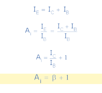
In this type of configuration, the current flowing out of the transistor must be equal to the currents flowing into the transistor as the emitter current is given as Ie = Ic + Ib. Also, as the load resistance (RL) is connected in series with the collector, the current gain of the common emitter transistor configuration is quite large as it is the ratio of Ic/Ib and is given the Greek symbol of Beta, (β). As the emitter current for a common emitter configuration is defined as Ie = Ic + Ib, the ratio of Ic/Ie is called Alpha, given the Greek symbol of α. Note: that the value of Alpha will always be less than unity. Since the electrical relationship between these three currents, Ib, Ic and Ie is determined by the physical construction of the transistor itself, any small change in the base current (Ib), will result in a much larger change in the collector current (Ic). Then, small changes in current flowing in the base will thus control the current in the emitter-collector circuit. Typically, Beta has a value between 20 and 200 for most general purpose transistors. By combining the expressions for both Alpha, α and Beta, β the mathematical relationship between these parameters and therefore the current gain of the transistor can be given as:

Common Collector Configuration: CC
In the Common Collector or grounded collector configuration, the collector is now common through the supply. The input signal is connected directly to the base, while the output is taken from the emitter load as shown. This type of configuration is commonly known as a Voltage Follower or Emitter Follower circuit. The emitter follower configuration is very useful for impedance matching applications because of the very high input impedance, in the region of hundreds of thousands of Ohms while having a relatively low output impedance.

The common emitter configuration has a current gain approximately equal to the β value of the transistor itself. In the common collector configuration the load resistance is situated in series with the emitter so its current is equal to that of the emitter current. As the emitter current is the combination of the collector AND the base current combined, the load resistance in this type of transistor configuration also has both the collector current and the input current of the base flowing through it. Then the current gain of the circuit is given as:
Common Collector Current gain:
Thank You
No comments:
Post a Comment